Published by Stanisław GALLA, Arkadiusz SZEWCZYK,
Gdansk University of Technology Faculty of Electronics, Telecommunications and Informatics
Abstract. In the paper authors present results of observation of input power changes versus harmonics amplitude in supply voltage of low-power power supply device. In the study, the electrical measurements supported with thermal imaging were used. The input circuit elements of studied device responsible for input power increase are pointed.
Streszczenie. W artykule przedstawiono wyniki pomiarów zmian mocy wejściowej pobieranej z sieci zasilającej przez zasilacz małej mocy w funkcji harmonicznych napięcia zasilającego. Wytypowano elementy obwodu wejściowego badanego urządzenia odpowiedzialne za zwiększenie poboru mocy przy zasilaniu napięciem silnie zniekształconym. W badaniach oprócz pomiarów elektrycznych wykorzystano również obrazowanie termograficzne. (Pomiar parametrów mocy wejściowej zasilacza zasilanego przez napięcia odkształcone zaburzeniami niskich częstotliwości).
Keywords: power supply, distortions, measurements.
Słowa kluczowe: zasilacze, zaburzenia, pomiary.
Introduction
Main parameters that describe electronic equipment declared by producer are, among of others, supply voltage, current consumption, working frequency and efficiency. Producer by declaring values of parameters guarantees that in standard working conditions their values will be in specified range. For equipment intended for domestic use, values of those parameters are determined for standard supply conditions, that means the supply voltage is sinusoidal with specified frequency and amplitude (RMS value). However, in real supply nets the voltage is disturbed by low and high frequency components, what was described e.g. in [1, 2, 3, 4]. For low frequency range, the one of parameters that describes the quality of supply voltage is total harmonics distortion (THD). The methodology of THD estimation and its maximum values are briefly described in several international standards [5, 6]. Currently, it is presumed that in public low voltage supply nets the THD value should not exceed 8%. Unfortunately, significantly higher values of THD are registered in several supply subnets and can have harmful influence on electric and electronic equipment that is supplied with such a voltage. The example influence of disturbed supply voltage on electronic apparatus, which is switching power supply is described in this report.
Issue consideration
The considered problem was reported by one of the electronic equipment producer. The user of low-power (<70 W) switching power supply reported significant discrepancy between supply current value he recorded and the value declared in technical note. The user pointed also differences in values of other parameters measured for nominal load. During the work on the problem, it was recognized that even though the supply voltage was 230 VRMS (+5 VRMS / -7 VRMS) it was strongly distorted by harmonics. Conducted measurements showed that THD value reached 11% and both even and odd harmonics was observed. Atypically, the dominant 4th and 8th order harmonics were observed. It’s worth to mention here, that for low-power power supply sources the power ratio correction circuit is not required. The mentioned power supply source was then examined in laboratory conditions.
Experiments
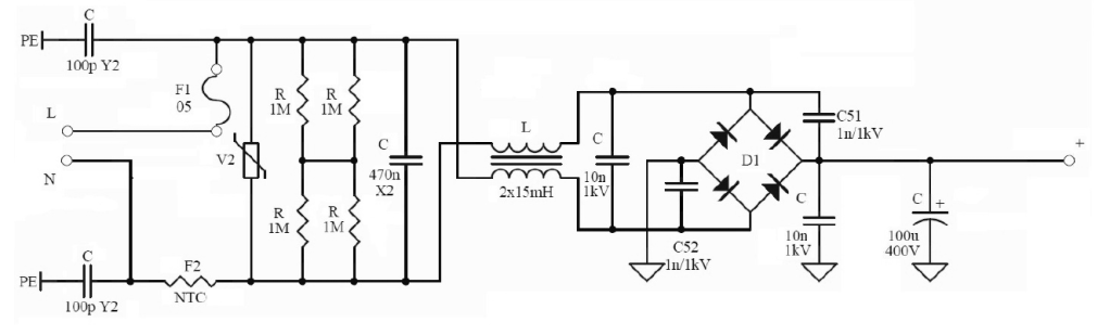
In order to examine the influence of each particular harmonic on device behaviour, the device under test was supplied with voltage distorted with harmonic (one at a time) which amplitude exceeded acceptable value specified e.g. in standard [4] and the current consumption was monitored. The device under test was 60 W switching power adapter with following parameters: nominal supply voltage Un = 230 V, nominal power P = 60 W, input current InRMS = 0.6 A, nominal output current, Io = 3 ADC, nominal output voltage Uo = 18 VDC. Producer guarantees 20% of parameters accuracy, according to appropriate standards. Figure 1 shows the input circuit of the device.
Measurement set-up
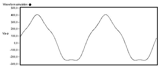
Examined device was supplied by CHROMA 61502 programmable AC source. The output RMS voltage of the AC source was URMS = 230 V (+/- 1%). The 50 Hz component of the output voltage was U1RMS = 228,8 V and was constant during the test. The RMS value of each harmonic component was UnRMS = 23 V, for n = 2 to 40 and the phase shift of the component was 90 degree. Figure 2 shows example test waveform for n = 4 (main component with 4th harmonic).
During the test, the device was loaded with the constant current Io = 3 A which gives output power Po = 54 W by electronic load Array 3721A. Under all test input and output parameters was monitored. Measured input parameters are: root mean square value of input voltage in frequency range 50 Hz – 2 kHz (URMS), root mean square value of input current in frequency range 50 Hz – 2 kHz (IRMS), peak current (Ip), real power (P), reactive power (Q), apparent power (S), peak current (IP), power factor (PF), crest factor (CF).
During the measurement, the device under test was also observed by thermographic camera VIGO V50. The camera has spectral range of 8 μm to 14 μm and 384 x 288 pixels resolution. The camera was equipped with 15o x 11o lens [7]. Registered thermal images allowed for identification of circuits and components responsible for elevated power consumption by the device under test. First, the thermal image of the DUT was registered for pure, 50 Hz supply, with no harmonics. Next this image was compared with thermal images taken for power supply disturbed by harmonics. Images was taken in thermal equilibrium state, when the temperature of the DUT’s components was stable.
Results and discussion
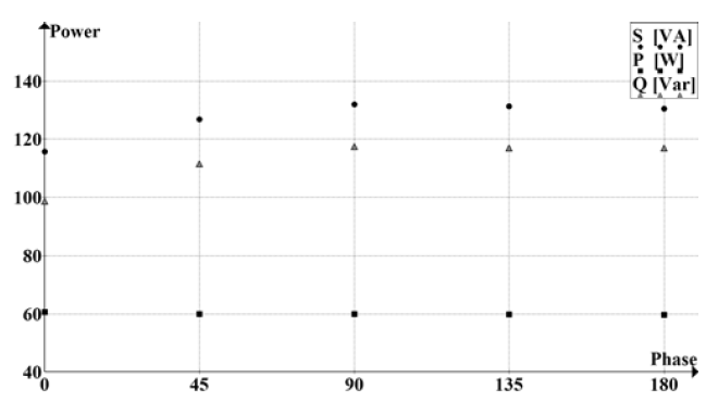
Figure 3 shows real, reactive and apparent power for each harmonic. The increase in reactive and apparent power is observed for low order harmonics. Moreover, the more significant increase is observed in case of presence of even harmonics.
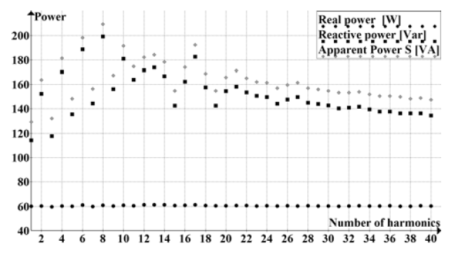
The maximum increase, up to 210 VA is observed for 8th harmonic, while for not disturbed voltage the value is about 120 VA. For higher harmonics, above 25th , the difference in influence of even and odd harmonics is not significant and both reactive and apparent power decrease.
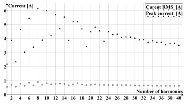
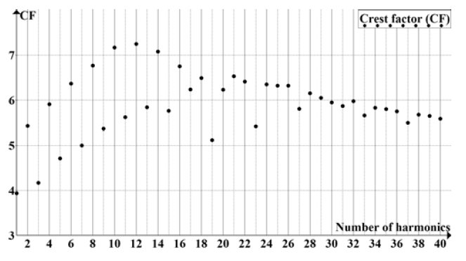
Figure 4 and 5 show input current (RMS and peak value) and crest factor respectively. Both RMS value of current and crest factor corresponds to power consumed by tested circuit.
Additionally, the influence of phase shift between fundamental component and harmonic was studied. Figure 6 shows the change in value of real, reactive and apparent power for 3rd harmonic. Received data shows that the influence of phase shift of the harmonic on power lost in device is less than 20% (+/- 10%) and can be treated as being in tolerance of parameters specified by producer.
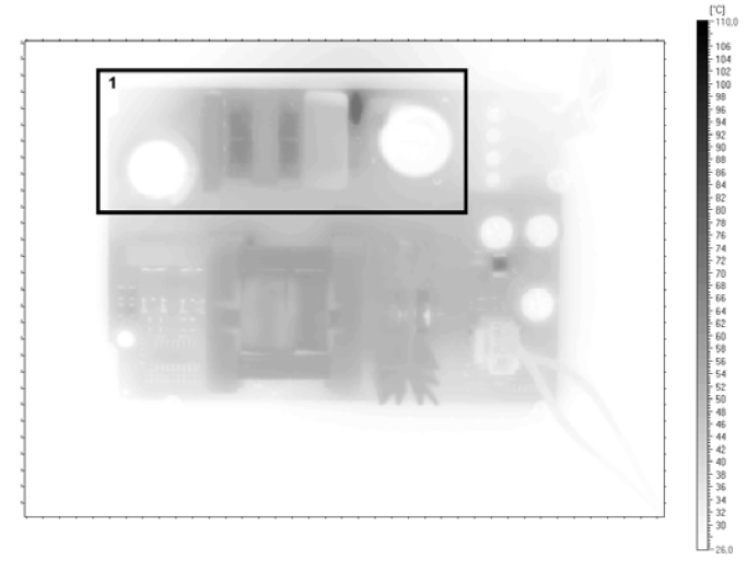
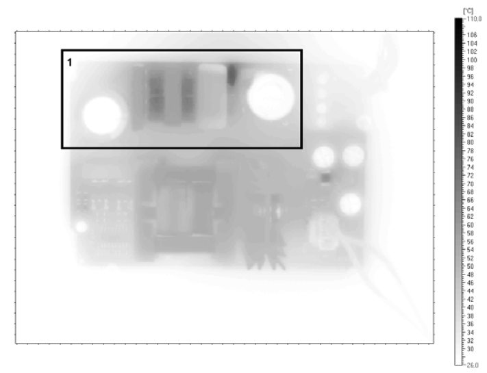
During the test, the temperature of device’s circuit board was monitored using thermal imaging camera VIGO v50. Figure 7 shows thermal image of DUT’s circuit board when supplied with not disturbed supply voltage (with no harmonics added).
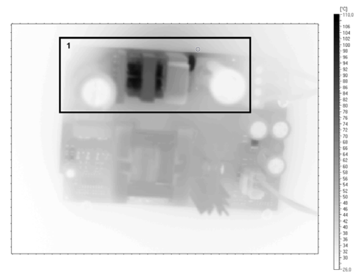
Figure 8 shows thermal image of DUT’s circuit board when powered with supply voltage disturbed by 8th harmonic, while figure 9 shows the one for 11th harmonic. As is seen in figures 3, 4 and 5, for the 8th harmonic the maximum input power and for 11th one the maximum value of crest factor are observed.
Comparing thermal images stored for various supply conditions allows to point out regions and components, where the energy is lost in a form or heat radiation.
In our case the main temperature increase is observed in compensated choke, L (2 x 15mH). Increase of temperature of input filters circuit points, that the energy is lost there and for even harmonics the temperature of filter elements is twice higher than for odd harmonics.
Conclusions
Conducted measurements confirmed observation results reported by the device user. In specific supply conditions when the supply voltage is strongly disturbed, device parameters value can be significantly out of range given by producer. It’s worth to mention here, that in standard supply conditions device parameters are within the specified range. In most supply nets, the voltage is distorted mainly by odd harmonics, for which the observed increase in reactive and apparent power is much lower than for even ones. The device user should take appropriate steps to decrease disturbances in his supply net and its adverse influence on various electric devices.
Observed enormous increase in power consumption caused by even harmonics results in increase of input circuit elements temperature. That thermal exposure can lead to decease of device reliability. It should be taken into consideration by producers if it’s worth to evaluate device parameters for maximum negative supply conditions, e.g. for maximum distortion values specified in appropriate standards.
Nevertheless, it should be stated here, that the input filter circuit of examined supply device is not chosen fortunately. It meets restrictions pointed in standard [6] for class B devices in terms of conducted emission, while used inductive element (inductive choke) shows increased thermal emission and cause increase in input power, especially for even harmonics distortions.
REFERENCES
[1] Łuszcz J., Oddziaływanie przekształtników energoelektronicznych dużej mocy na jakość energii elektrycznej, Zeszyty Naukowe Wydziału Elektrotechniki i Automatyki, Nr 31/2012, 211-214
[2] Hanzelka Z., Jakość dostaw energii elektrycznej. Zaburzenia wartości skutecznej napięcia. Akademia Górniczo Hutnicza, 2013
[3] Shafiul I. M, Chowdhury N., Sakil A. K., AtifIqbal K.A., Abu-Rub H., Power Quality Effect of Using Incandescent, Fluorescent, CFL and LED Lamps on Utility Grid, 978-1-4673-6765-3/15
[4] Blackledge J., O’Connell K., Barrett M., Sung A., Cable heating effects due to harmonic distortion in electrical installations, International Association of Engineers: ICEEE12, London, 2012
[5] PN-EN 50160:2010, Parametry napięcia zasilającego w publicznych sieciach elektroenergetycznych
[6] EN 61000-4-30:2015 Electromagnetic compatibility (EMC) – Part 4-30: Testing and measurement techniques – Power quality measurement methods
[7] http://www.vigo.com.pl/pub/File/PRODUKTY/Thermal-imagingsystem/v50.pdf, dostęp z sieci PG: 2016.06.13
Authors: dr inż. Stanisław Galla, Politechnika Gdańska, Wydział Elektroniki i Informatyki, Katedra Metrologii i Optoelektroniki, ul. Narutowicza 11/12, 80-233 Gdańsk, E-mail: galla@eti.pg.gda.pl;
dr inż. Arkadiusz Szewczyk, Politechnika Gdańska, Wydział Elektroniki i Informatyki, Katedra Metrologii i Optoelektroniki, ul. Narutowicza 11/12, 80-233 Gdańsk, E-mail: szewczyk@eti.pg.gda.pl
Source & Publisher Item Identifier: PRZEGLĄD ELEKTROTECHNICZNY, ISSN 0033-2097, R. 92 NR 11/2016. doi:10.15199/48.2016.11.07
