Published by Saktanong WONGCHAROEN, Sansak DEEON, Pathumwan Institute of Technology, Thailand
Abstract. This article presents the application of a multi-stage window comparator circuit with safety mode for swell voltage control in low voltage systems that lack stability and electrical quality. High-voltage transistors were used to build a simple voltage detecting circuit with multi-stage functions and electronic load to detect and control swell voltage . SVSS as the overloaded energy receptor resulted in clamping voltage. The voltage of a device is equal to the voltage flowing to smart electronic loads and not over the IEEE 1159 and 1100 standards. The device worked normally without causing damages. Failure Mode and Effect Analysis (FMEA) might occur using a multi-stage window comparator circuit in the safety mode. The reliability and stability in detecting voltage and controlling electronic loads to work safely under many kinds of situations were also assessed.
Streszczenie. W artykule zaprezentowano wykorzystanie komparatorów do kontroli zwiększonego napięcia w systemach niskiego napięcia. Napięcie nie przekracza zaleceń norm IEEE 1159 i 1100. Zastosowanie kaskadowych komparatorów w trybie bezpieczeństwa do kontroli spiętrzenia napięcia w systemach niskonapię1)ciowych
Keywords: window comparator multi-stage, Failure Modes and Effects Analysis (FMEA), Swell Voltage Surge Suppressor (SVSS)
Słowa kluczowe: komparatory kaskadowe, analiza zakłóceń pracy układu, przepięcvia.
Introduction
Advancement of electronic technology has resulted in many innovations that facilitate and improve the lives of people. For example, information and knowledge can be easily accessed by connecting to the internet, building smart homes, smart grids, solar PV rooftops [1] and smart farms. Smart electronic devices are now connected to the distribution system in the Provincial Electricity Authority (PEA). These advanced technological electronic devices have sensitivity towards noise. Quality problems of electricity systems or swell voltage cause damages to smart electronics used in the household as seen in Fig. 1.
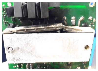
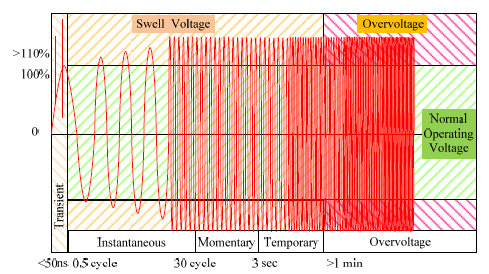
Problems of electric quality are often found in rural areas caused by lighting, switched capacitors, system maintenance, use of nonlinear devices, incorrect ground system and use of inconsistent technology in the electrical system [2-3]. These problems promote changes in electrical quality. If the devices have sensitivity towards the response this might cause failure or malfunction. Although many systems have Surge Protection Devices (SPDs) for AC surge [4-7], damage to electronic devices still occurs as seen in Fig. 1. Damages from the change of electrical quality or swell voltage occur when RMS voltage exceeds IEEE 1159 and 1100 standards [8-9] (Fig. 2). Installation of SPDs in low-voltage systems [10] cannot prevent swell voltage lower than the working level of the device, resulting in damages to smart electronic machinery. This is a big problem for electrical quality of distribution systems in PEA. Apart from the damages, swell voltage also impacts users. As a result, analysis and improvement of electrical quality must adhere to real situations of specific areas in the country.
This article presents the concepts of application of a multi-stage window comparator circuit with safety mode for swell voltage control in low voltage systems through the development of a Swell Voltage Surge Suppressor (SVSS) to reduce damages to smart electronic devices conducted to distribution systems in PEA. Design of a multi-stage window comparator circuit with safety mode using high-voltage transistors [11-14] enhances the endurance of the circuit towards high voltage systems and prevents failure, resulting in improved circuit reliability.
Basic Window Comparator Circuit
Window comparator circuits (WCs) often used are IC Op-Amp, Logic gate, IC packet, IC CMOS and TTL [15-18]. The window comparator circuit type IC has low input voltage and current. It is suitable for analysing small signals. If devices inside the IC are damaged or lack qualification, the circuit will not work or work abnormally. For these IC devices, characteristics of damages inside the circuit cannot be examined. The window comparator circuit has different low-voltage levels (VLow) and high-voltage levels (Vhigh). This qualification is called Hysteresis and is used to detect the signal as the designed function. If the analogue input (Vin) is in the range of standardised electrical level, the output signal will be 1 (High). However, apart from this condition, signal output will be 0 (Low).
Window Comparator Circuit with Transistors
After the IC window comparator circuits have been applied to detect the overvoltage [19], this might damage the devices inside IC. The use of transistors in the design of window comparator circuits is important [12-14]. Today, semi-conductors have been developed for use at higher voltage. Application of high-voltage transistors with VCE ±300V of KSP42 and KSP92 transistors in the design can be adapted for other uses. Oscillator circuits made from a pair of transistors are used in window comparator design (Fig. 3). When Vin is higher than Vref_L (Vin>Vref_L), the transistor Q1 works (on) with electricity flowing through Q1, resulting in clamping voltage at R3 (VR3). The resistors, R4 and R5, are voltage divider circuits. They control the function of low voltage (Vref_L) as seen in the equation.
When Vin has voltage higher than Vref_H (Vin>Vref_H), the transistor Q2 will work (on) while the resistors, R1 and R2, which are voltage divider circuits, control the function of low voltage (Vref_H). When the transistor Q2 works and enters saturation, the output signal Vout =0V as seen in the equation.
Application of a window comparator circuit requires expansion of the output signal to make the output signal logic become 0 (OFF) or 1 (ON). When Vin is at the specified level, the voltage Vout at the Q3 transistor’s base is around 0.7V, resulting in electricity flowing and the clamping voltage Vce of the Q3 transistor is 0V. The Q4 transistor will not work (IC =0). Therefore, the transistor works like a switch in an open circuit or in the cut-off state, causing clamping Vce(cut-off) at the Q4 transistor equal to Vo and VP as seen in the equation.
When Vin is outside the standard voltage level, the voltage at the Q3 transistor’s base will be lost, causing flow of electricity (IC=0). The clamping voltage has R6 equal to ICR6, resulting in voltage at the Q4 transistor’s base while the electricity IC flows to the high position resulting in clamping voltage Vce=0V. Therefore, the transistor works like a switch in a closed circuit or in saturation state as seen in equation.

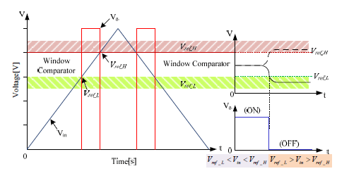
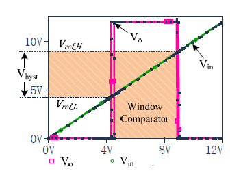
In Fig. 4, Vp is the output voltage that can control the voltage level of electronic loads. Characteristics of the output signal of a window comparator circuit with Q3 and Q4 transistors work like a switched circuit. When the signal of Vin in the windows of Vref_L and V ref_H is according to the set function as seen in Fig. 5, the output signal remains High (ON). If Vin is outside of Vref_L and V ref_H, the output signal will be Low (OFF) as seen in the equation.
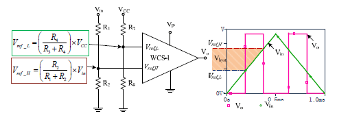
To make it simple, a block diagram similar to Op-amp was drawn with single input and output. This means 1 Opamp symbol is equal to 1-stage window comparator circuit or WCS-1 as seen in Fig. 6.
From Fig. 6, set the function of window comparator with four resistors: R1, R2, R3, and R4, connecting in the voltage divider circuit as R1 and R2 to control the function of Vref_H while R3 and R4 control the function of Vref_L. To create the signal channel of the window comparator, the difference between voltage level Vref_L and Vref_H will be called hysteresis voltage or Vhyst [18]. This could cause a change of voltage level at two positions as seen in Fig. 7. Consequently, to calculate Window Comparator Hysteresis, the voltage level should be set to eliminate the swing of the input signal Vin due to error or noise as the equation below.
Multi-stage Window Comparator Circuit
A multi-stage window comparator can set multi ranges of voltage level to assess the difference between Vref_L-N and Vref_H-N when an analog output signal Vin is added into the system. If it is from WCS-1 to WCS-N as the regulated function, the output signal from Vo-1 to Vo-N of any stage will be 1. Apart from this condition, the output signal will be 0 as seen in Fig. 8.

Fig. 8 demonstrates the overview of the multi-stage window comparator circuit. When used to detect swell voltage, it will assist by dividing the violent level of swell voltage that enters the low voltage system. Selection of device, resistor and transistor in the circuit must be endurable. The working function must be examined and failure mode analysed to check the abnormality of physical characteristics.
Principle of Swell Voltage Control
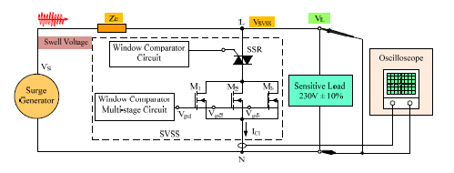
Swell voltage control by a Swell Voltage Surge Suppressor (SVSS) can be used as the electronic load that receives overvoltage in the system [20-21]. There are four sets of window comparator circuits for detecting swell voltage. Each set has a different window level. WCS-1 first detects the swell voltage. If Vin shares the same value as the window’s voltage of WCS-1, the output signal Vo1 becomes 1. When Vin rises to reach the window levels of WCS-2, WCS-3 or WCS-4, then one of the output signals at Vo2, Vo3 or Vo4 is 1. All three sets work under the window level of WCS-1 as seen in Fig. 9.
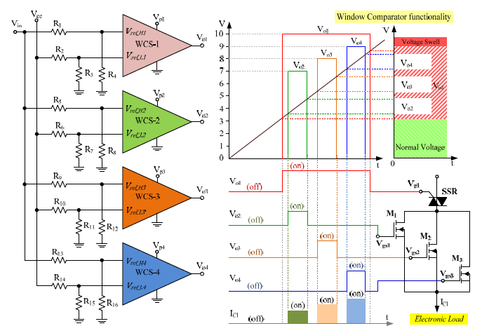
In Fig. 9, the electronic load controlled by the multi-stage window comparator circuit will work when Vin shares the same window level as WCS-1. The output signal Vo1 will force the switch of Solid-state Relay (SSR) [22] to activate (on) and when the voltage of Vin is equal to the window level of WCS-2 ,WCS-3 or WCS-4, it will cause Leakage Current (LC1) through electronic loads M1, M2 or M3, which connect in parallel. If the device at M1 level becomes damaged and the voltage Vin continues to increase, M2 and M3 still work. M1, M2, and M3 are electronic device type Power MOSFET. Here, selected SCT3080KL MOSFET with voltage between Drain– Source could reach 1,200V. It is an electronic lead that works as the energy supporter and could be compared to a load in the system. The use of MOSFET enhances the endurance of the electronic circuit to be safer, more constant and prevent dangerous failure that might occur in the system. When Vin is lower, the window comparators WCS-2 , WCS-3 or WCS-4 will cause M1, M2 or M3 to stop working, while they are working under WCS-1, until the voltage is lower than WCS-1. It also causes the SSR to stop working (off). The electricity IC1 ceases to flow. Characteristics of electronic load control of M1, M2, and M3 have different voltage control level. This affects the flow of electricity through electronic loads and helps to control the loaded voltage at the standard level in accordance with IEEE Std 1159 and IEEE Std 1100.
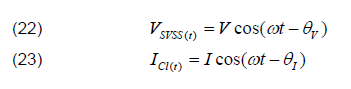
The multi-stage window comparator for swell voltage control with RMS over the standard (230V ±10%) [8-9] will be installed parallel to the power system. The swell voltage causes electricity to flow through the first rectifier circuit, which is the voltage sensor (VSS), while the resistors R1 and R2 connect to the voltage divider circuit to reduce the voltage to remain at the appropriate level. The received Vin will be added to the window comparators WCS-1 WCS-2 WCS-3, and WCS-4 respectively, as seen in equation.

From Fig. 10, the voltage detector circuit by the window comparator with the safe mode will examine the voltage Vin. If Vin follows the condition, the output signals Vo1, Vo2, Vo3 or Vo4 will control electronic loads in accordance with the overvoltage level in the system. The electronic load control circuit will supply electricity and control voltage, resulting in clamping voltage at the electronic loads as seen in the equation.

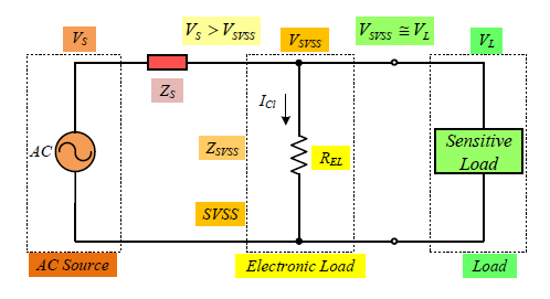
If drawing the block diagram by replacing SVSS as the resistor load (REL), when removing the sensitive load out of the circuit, it is evident that REL makes the series with the resistant (ZS) of the power distribution source by dividing from the voltage at VSVSS. As seen in Fig. 11, the electronic load pulls the power current ICl to flow through itself as a means to preserve the voltage level, VSVSS ≅ VL that is distributed to the load to remain level and not over the standard as seen in the equation.
The electronic load is similar to the resistor load connecting to the AC source, resulting in swell voltage and swell current as seen in the equation.
To calculate the clamping voltage of the electronic load circuit, see the equation.

For consideration of the power of electronic loads in the AC power system during the electricity flow due to swell voltage, the multiple results of voltage and short current, see the equation.
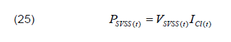
Table 1. Result of Failure Modes and Effects Analysis of the created Window Comparator Circuit
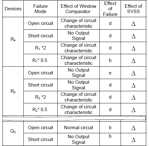
Notes *(0.5) and *(2) referred from the standard measurement. (a): Normal Output (b): No Output (c): window Voltage reduced (d): window Voltage increase (e): Output as Vp (f): Half reduction output Δ : no significant consequences of SVSS
Analytical Result of The Window Comparator’s Safe Mode Circuit
Failure Modes and Effects Analysis (FMEA) [23-26] is the indicator in analysis of the safe failure of the window comparator that leads to prevention of damages. The principle of the analysis has been standardised and the result confirms that the window comparator circuit will work with the safe mode. If there is any dangerous failure with any device in the window comparator or the four sets, SVSS will stop working immediately and will not cause any dangerous failure to the system. See Table 1.
Testing Result of Swell Voltage Control
The SVSS device was tested for swell voltage control [27-29] by connecting to the top the system before distributing the voltage at 280V, 290V, 300V, 310V, 320V, 330V, 340V and 350V [20-21] and measuring the signal wave of clamping voltage at the output as seen in Fig. 12 and Fig. 13.

The wave of the output signal of the multi-stage window comparator was measured for electronic load control by adding the triangle-wave signal to test its function. When the voltage reached the destined level, the output signal through the windows Vo1, Vo2, Vo3, and Vo4 to control the electronic loads in accordance with the overvoltage. See Fig. 14 and Fig. 15.

The distributed AC current was at 280-350V and the frequency was 50 Hertz. The wave of the signal to test the size of overrated voltage is shown in Fig. 16. The test applied an oscilloscope to measure the signal wave of current and clamping voltage at the output before recording (Table 2).

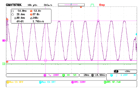
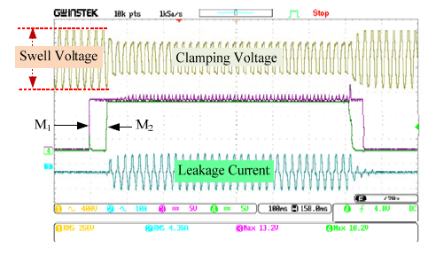

Fig. 17 shows the distributed overvoltage in the system. The signal detected CH1 as the signal wave of swell voltage and CH3 as the output signal from the window comparator with V01 as the signal forcing M1 CH4 as the output signal from the window comparator with V04 as the signal forcing M2, and CH2 as the wave of electric current ICl flowing through the electronic loads for swell voltage control. as seen in Fig. 18 and Fig. 19.
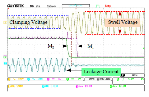
Table 2. SVSS Test Results for Swell Voltage Level Control
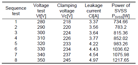
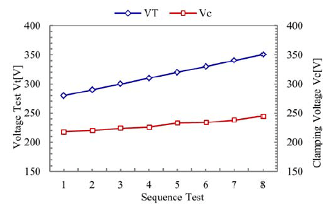
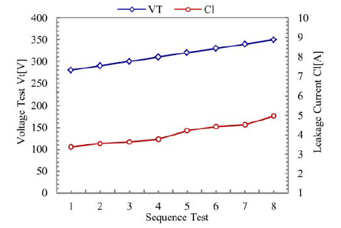
Data were demonstrated in the graph as the relationship between voltage, electric current and electric power of SVSS for swell voltage control as seen in Fig. 20, Fig. 21 and Fig. 22 respectively.
Conclusion
This article demonstrated the multi-stage window comparator circuit as safe for swell voltage control in low voltage systems. Problems are caused by the quality and stability of the power system and might affect smart electronic devices conducted on distribution systems in PEA. The design of swell voltage level control contains the main circuit as the window comparator circuit with safe mode to detect the overvoltage level from the high-voltage transistor, with the purpose of enhancing the endurance of high-voltage. It also reduces the effect of dangerous failure in the system. The created window comparator circuit can detect voltage level and control electronic loads with safe mode. The FMEA result based on IEC 61496-1 standard, assured the working process of the device to be reliable and stable to control safety under many kinds of situations. The testing result showed that SVSS for swell voltage level control was effective by allowing the electric current to flow through itself, resulting in reduction of voltage level. The current moving through smart electronic devices was not over the standards of IEEE Std 1159 and IEEE Std 1100.
REFERENCES
[1] SB. Kjaer, JK. Pedersen, and F. Blaabjerg, “A review of single-phase grid-connected inverters for photovoltaic modules,” in IEEE Transactions on Industry Applications, 41(2005), 1292–1306
[2] D. O. Johnson, K. A. Hassan. “Issues of Power Quality in Electrical Systems,” International Journal of Energy and Power Engineering, 5 (2016), No. 4, 148-154
[3] J. Kaniewski, “Transformator hybrydowy z dwubiegunowym przekształtnikiem AC/AC bez magazynu energii DC,” Przegląd Elektrotechniczny, ISSN 0033-2097, 94 (2018), nr 5, 80-85
[4] V. Radulovic, S. Mujovic, and Z. Miljanic, “Characteristics of Overvoltage Protection with Cascade Application of Surge Protective Devices in Low-Voltage AC Power Circuits,” Advances in Electrical and Computer Engineering, 15 (2015), No. 3, 153-160
[5] IEEE Std C62.41.1-2002, IEEE Guide on the Surge Environment in Low-Voltage (1000 V and Less) AC Power Circuits, April 2003.
[6] P. Hasse, Overvoltage Protection of Low Voltage Systems, 2nd ed. United Kingdom: The Institution of Electrical Engineers, 2000.
[7] D. Paul, “Low-voltage power system surge overvoltage protection,” in IEEE Transactions on Industry Applications, 37 (2001), 223-229
[8] IEEE Std 1159-2009, IEEE Recommended Practice for Monitoring Electric Power Quality, November 2009.
[9] IEEE Std 1100-2005, IEEE Recommended Practice for Powering and Grounding Electronic Equipment, December 2005.
[10] Z. He and Y. Du, “SPD Protection Distances to Household Appliances Connected in Parallel,” in IEEE Transactions on Electromagnetic Compatibility, 56 (2014), No. 6, 1377-1385
[11] E. J. Wade, and D. S. Davidson, “Application of Transistors to Safety Circuits,” in IRE Transactions on Nuclear Science, 5 (1958), No. 2, 44-46
[12] K. Futsuhara, and M. Mukaidono, “Application of Window Comparator to Majority Operation,” in The Nineteenth International Symposium on Multiple-Valued Logic, (1989), 114-121
[13] K. Futsuhara, and M. Mukaidono, “A Realization of Fail-safe Sensor Using Electromagnetic Induction,” in Conference on Precision Electromagnetic Measurements CPEM, (1988), 99-100
[14] M. Sakai, M. Kato, K. Futsuhara, and M. Mukaidono, “Application of Fail-safe Multiple-valued Logic to Control of Power Press,” in 1992 Proceedings The Twenty-Second International Symposium on Multiple-Valued Logic, (1992), 271-350
[15] P. Sagar, P. P. R. Madhava, “A Novel, High Speed Window Comparator Circuit,” in 2013 International Conference on Circuits, Power and Computing Technologies (ICCPCT), (2013), 691-693
[16] M.W.T. Wong, and Y. Zhang, “Design and Implementation of Self-Testable Full Range Window Comparator,” in Proceedings of the 13th Asian Test Symposium (ATS2004), (2004), 1-5
[17] S. Maheshwari, “Current Conveyor Based Window Comparator Circuits,” Advances in Electrical Engineering, (2016), 1-8
[18] V. A. Pedroni, “Low-voltage high-speed Schmitt trigger and compact window comparator,” in Electronics Letters, 41 (2005), No. 22, 1213-1214
[19] Y. Zhang and M.W.T. Wong, “Self-Testable Full Range Window Comparator,” in IEEE Region 10 Conference TENCON 2004, (2004), 262-265
[20] N. Mungkung, S. Wongcharoen, C. Sukkongwari, and S. Arunrungrasmi, “Design of AC Electronics Load Surge Protection,” in International Journal of Electrical, Computer, and Systems Engineering, ISSN 1307-5179, 1 (2007), No. 2, 126-131
[21] N. Mungkung, S. Wongcharoen, K. Chomsuwan, P. Nuchuay, K. Permsupsin and T. Yuji, “Electronics Load for Voltage Swell Protection,” in Conference on Embedded Systems and Intelligent Technology, (2008), 303-307
[22] R. N. Eldine, I. Amor, A. Massoud, and L. B. Brahim, “Smart Low Voltage ac Solid State Circuit Breakers for Smart Grids,” in Global Journal of Advanced Engineering Technologies, 2 (2013), No. 3, 71-79
[23] IEC Std 60812-2018, Failure modes and effects analysis (FMEA and FMECA), 3th ed. IEC International Standard, July 2018.
[24] C. Summatta, W. Khamsen, A. Pilikeaw and S. Deeon, “Design and Simulation of Relay Drive Circuit for Safe Operation Order,” in Conference on Mathematics, Engineering & Industrial Applications 2016 (ICoMEIA 2016), August 2016.
[25] S. Deeon, Y. Hirao, K. Tanaka, “A Relay Drive Circuit for a Safe Operation Order and its Fail-safe Measures,” in The Journal of Reliability Engineering Association of Japan, 34 (2012), No.7, 489-500
[26] S. Deeon, Y. Hirao and K. Futsuhara, “A Fail-safe Counter and its Application to Low-speed Detection,” in The Journal of Reliability Engineering Association of Japan, 33 (2011), No.3, 135-144
[27] IEC Std 61496-1, Safety of machinery-Electro-sensitive protective equipment-Part 1: General requirements and tests, IEC International Standard, April 2012.
[28] IEEE Std C62.41.1-2002, IEEE Guide on the Surge Environment in Low-Voltage (1000 V and Less) AC Power Circuits, April 2003.
[29] IEC Std 6100-4-5-2014, Electromagnetic Compatibility (EMC), Part 4-5, Testing and measurement techniques, Surge immunity test, IEC International Standard, June 2014.
Authors: Mr. saktanong wongcharoen, E-mail: saktanong.w@gmail.com; Dr. Sansak Deeon, E-mail: sdeeon2013@gmail.com. Department of Electrical Engineering, Pathumwan Institute of Technology, 833 Rama1 Wangmai District, Bangkok, Thailand;
Source & Publisher Item Identifier: PRZEGLĄD ELEKTROTECHNICZNY, ISSN 0033-2097, R. 96 NR 5/2020. doi:10.15199/48.2020.05.17
