Published by 1. Mariusz STOSUR1, 2. Kacper SOWA2, 3. Piotr ORAMUS1, 4. Adam RUSZCZYK2, 5. Pawel ALOSZKO3,
ABB E-mobility, Krakow, Poland (1), ABB Technology Center, Krakow, Poland (2), ABB Corporate Technology Center, Krakow, Poland (3)
ORCID. 1. 0000-0002-1522-3405, 2. 0000-0001-8246-2337, 3. 0000-0002-4810-3936, 4. 0000-0001-7477-8139, 5. 0000-0002-1668-6292
Abstract: This paper presents a hybrid switches based on semiconductors and mechanical switches. Devices are dedicated to limitation of adverse effect of capacitive type loads start-up especially in domestic applications, during which high value of inrush current is generated. Two different approaches are studied in the paper, both of them using energy harvesting to operate. The proposed solution combine together several advantages switches, such as: increased lifetime of the mechanical part, small on-state losses, smaller dimensions in comparison to mechanical switches, increased durability on overcurrent states, arc-less switching, or limited switching transients. In presented case solution is adopted as rocker switch of LED light sources.
Streszczenie. W artykule przedstawiono łączniki hybrydowe oparte na półprzewodnikach i łącznikach mechanicznych. Urządzenia przeznaczone są do ograniczania niekorzystnych skutków załączania obciążeń typu pojemnościowego, zwłaszcza w zastosowaniach domowych, podczas których generowana jest duża wartość krótkotrwałego prądu załączania. W artykule przeanalizowano dwa różne podejścia, z których oba wykorzystują do działania pozyskiwanie energii. Zaproponowane rozwiązanie łączy w sobie kilka zalet wyłączników, takich jak: zwiększona żywotność części mechanicznej, małe straty w stanie załączenia, mniejsze wymiary w porównaniu do wyłączników mechanicznych, zwiększona trwałość w stanach nadprądowych, czy ograniczenie łączeniowych stanów przejściowych. W prezentowanym przypadku przyjęto rozwiązanie jako łącznik kołyskowy źródeł światła LED. (Ograniczenie wpływu krótkotrwałego prądu załączania w zastosowaniach inteligentnych budynków).
Keywords: inrush current, transient state, arcing, mechanical contacts, hybrid switches
Słowa kluczowe: krótkotrwały prąd załączania, stany przejściowe, łuk elektryczny, zestyki, łączniki hybrydowe
Introduction
Traditional and mechanical switches find an application in electric circuits which are used in many branch of an industry and in residential installations [1-2]. The proper functioning of mechanical switching apparatus depends on surface conditions of electrical contacts. It should be also emphasized that, the electrical contacts are a part of an electrical switch, which is the most responsible for its proper functioning.
Moreover, the design of the electrical contacts must be resistant for phenomena such as: a mechanical abrasion, an oxidation and a corrosion, contact welding, heating and a temperature rise. The electric arc erosion of the contacts also happens due to inrush current during switching operation – especially during turning on LED light lamps, which are perfect example of capacitive type of the loads.
For these reasons, limiting arc erosion is important issue. The limitation of the electric arc erosion maintains the surface of electrical contacts in good conditions for longer time which, as a consequence, causes an increase of lifespan of entire switch. Hence, the limitation of the electric energy and the electric arc erosion is an important issue to provide a high reliability of electricity transmission in electrical circuits [3-4].
One of the most effective method proposed in this note for limiting electric arc energy is application of hybrid switch. Basically, hybrid switches connect many advantages of mechanical and semiconductor switches, such as: increased lifetime of the switch, small on-state losses, smaller dimensions in comparison to mechanical switches, increased durability on overcurrent states, arc-less switching, or limited switching transients. Idea presented in this document helps to limit arc erosion during light switching-on operations [5-7].
Despite that hybrid constructions being combination of mechanical and semiconductor switches are devices known from many years, the proposed idea includes new method for control of semiconductor part. Thanks to this, a design and overall complexity of entire hybrid switch is significantly simplified.
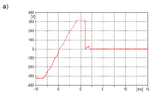
Modern LED sources of light are typical capacitive type of loads, connected to the mains through single-phase rectifier (Graetz bridge). Electrical diagram of LED bulb driver is illustrated in Fig. 1a.
In such a circuit an inrush current will always occur, when capacitor will be fully discharged and switching instance occurred in non-zero crossing of line voltage, in accordance with formula (1):
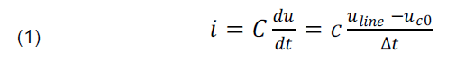
where: C – the value of capacitance; uline – instantaneous value of line voltage; uc0 – value of capacitor voltage.
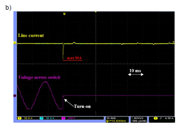
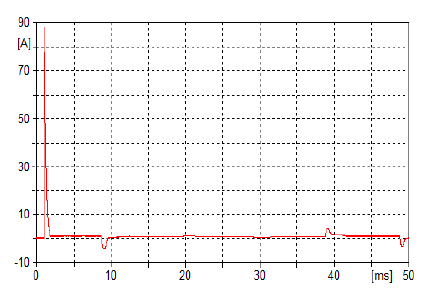
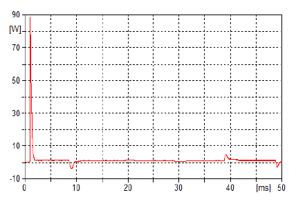
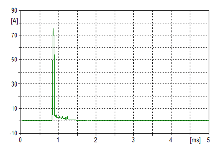
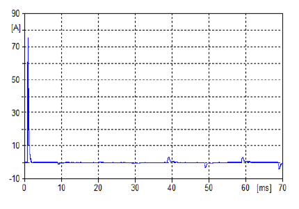
According to formula (1) the highest value of the current will occur when: uline = max and uc0 = 0 V (turning on in maximum of line voltage when capacitor is fully discharged). Such a case (current recorded during turning on LED lamps) is illustrated in Fig. 1b. Initial value of the current for 8 bulbs (8 × 11 W) can even exceed 90 A.
This paper presents two different methods of inrush current limitation. The first one based on triac semiconductor switch connected with two mechanical switches working in defined sequence during switching operation and the second one based on MOSFET semiconductor switch connected into the operated switch.

Application of hybrid switching allows to achieve almost completely arc-less and limiting inrush current through application of synchronized switching (the current starts to flow in circuit at voltage zero-crossing). This approach significantly increases reliability of the switch in comparison to traditional mechanical switch. Development of low voltage hybrid switch (using triac semiconductor elements) with increased lifetime could be interesting for household and industry applications.
Principle of operation of proposed hybrid switches
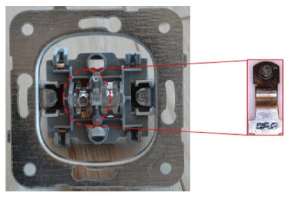
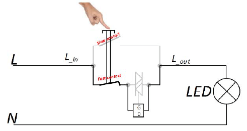
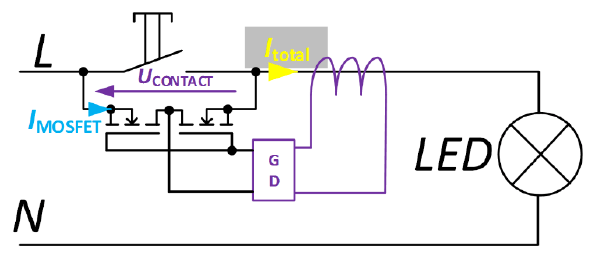
Currently, LED lights may cause a welding of a conventional light switch contacts and their erosion (inrush current effect during switching operation), which introduce accelerated aging and reduction of switch lifetime and reliability (Fig. 2). The presented idea increases lifetime of light switches by means of application of semiconductor components. During switching operation, current starts to flow at voltage zero-crossing, and almost entire current commutates into semiconductor branch, which significantly helps to keep mechanical contacts of the switch in good conditions for long time. Basic principle of operation for Zero Voltage Switching (ZVS) switch is presented in Fig. 3.
1. Triac solution
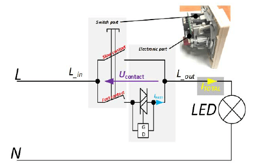
This solution comprises double mechanical contact switch with coupled drives in defined way (connected together through dedicated cam). Proposed solution provides defined time delay (≥ 10 ms) between closing both switch contacts (called further “slow” and “fast” contact). According to Fig. 3. The semiconductor branch is connected in series with fast switch and in parallel with the main switch (slow contact), which provides galvanic insulation of interrupting circuit.
Switching sequence of proposed device is as following:
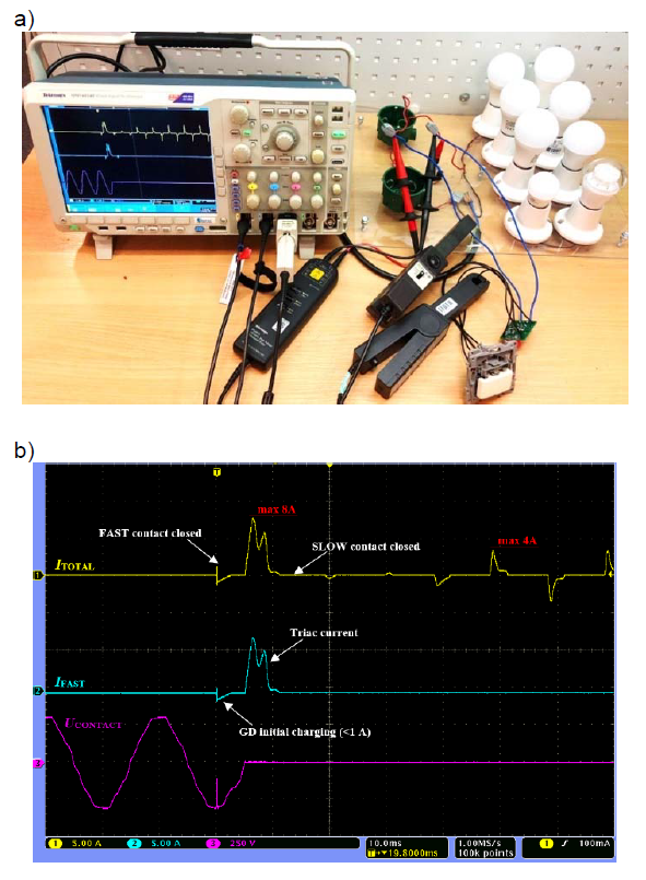
(I) Drive of the switch is pushed by pressing it, which first resulting in closing of fast switch. As a result, energy from energized circuit is harvested by triac gate-driver (GD), which is composed of single-phase rectifier with capacitor (detailed electrical diagram is depicted in Fig. 6a). The capacitor is fully charged within 5 ms, which allows to prepare triac for starting conduct current. Current patch during sequence is illustrated in Fig. 4.
(II) When the level of the energy stored in capacitor is sufficient and the nearest zero voltage crossing occurred, triac is ignited by optotriac module. This leads to significant limitation of inrush current value. The level of the energy stored in capacitor provides triac ignition for several periods of line voltage. Current patch during this sequence is illustrated in Fig. 5.

(III) In the final step branch witch thyristors is bypassed by slow contact, hence current commutated to branch with lower loses and triac is turned off as illustrated in Fig. 6. Time between closing of slow and fast contacts is above 10 ms.
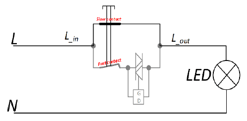
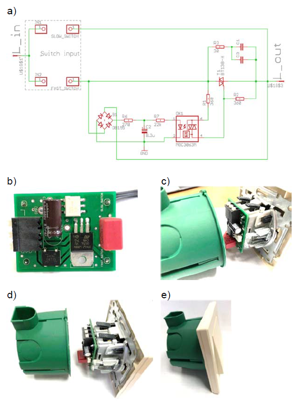
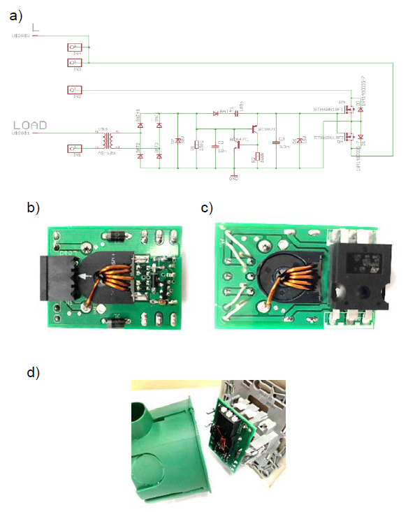
Diagram of the circuit and designed in Autodesk Eagle PCB integrated with light switch are presented in Fig. 7. The size of the PCB allows direct integration with existing solutions of the switches.
Experimental verification has been carried out in circuit depicted in Fig. 8a with several types of LED bulbs (different manufacturers). Voltage across switch and two currents have been recorded. A description of the oscillograms depicted in Fig. 8b is in accordance with switching sequence. Initial value of current has been significantly reduced – from 90 A (Fig. 1b) to 8 A (Fig. 8b), that is more than 11 times.
2. MOSFET solution
The second of proposed ideas is based on mechanical rocket switch which is bypassed by semiconductor switches (e.g. MOSFET’s), as illustrated in Fig. 9.
The mechanical contacts of the switch are normally opened and electric circuit is off (LED light is off). After mechanical contacts closing operation, di/dt (inrush current) is generated, due to LED light capacitance charging.
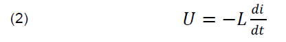
High di/dt is caused by voltage induction in primary winding of current transformer in accordance with formula (2):
Hence, di/dt impulse is responsible for generation of energy pulse which triggers the MOSFET’s, that bypass the mechanical contacts during closing or opening operation (in other words the MOSFET elements are bypassing current from mechanical contacts during “closing/opening operation”. Diagram of the circuit and designed PCB integrated with light switch are illustrated in Fig. 10.
Experimental verification has been also carried out in circuit depicted in Fig. 8b with several types of LED bulbs. Two currents have been recorded as illustrated in Fig. 11, MOSFET branch current and main switch current.
3. Measured and calculated waveforms
In this section, measured waveforms are presented for three different cases:
• circuit was energized by standalone mechanical switch,
• circuit was energized by hybrid switch based on MOSFET,
• circuit was energized by hybrid switch based on triac.
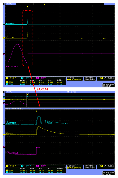
The magnitudes were measured according to simplified circuit diagram with marked measurement points in Fig. 12: the waveforms of currents (current of entire switch A1, current of semiconductor branch A2, current of mechanical contacts A3) and voltage across the switch during energization V. The waveforms are presented in sections 1- 3 for three considered cases.
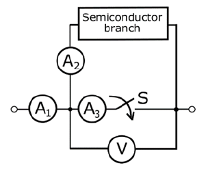
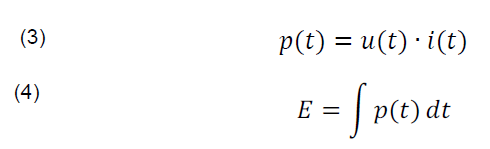
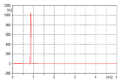
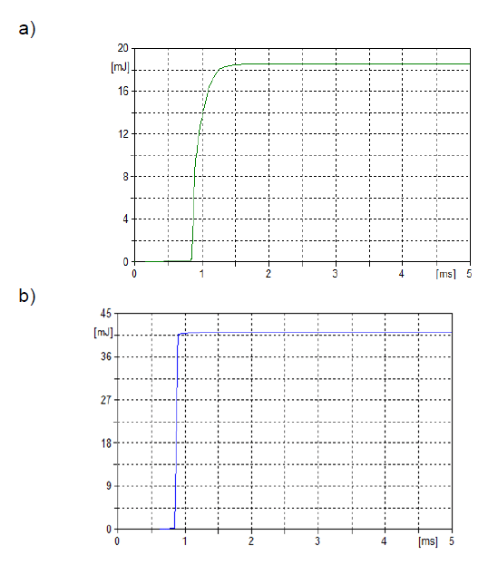
Based on measured voltage and currents, the following magnitudes were calculated: the power of LED energized by semiconductor branch, power of LED energized by mechanical contacts, amount of energy dissipated at semiconductor branch and amount of energy dissipated at mechanical contacts. The power and energy during energization process were calculated according to formulas (3) and (4).
Calculated waveforms are also presented in points 1÷3.
1. Standalone switch
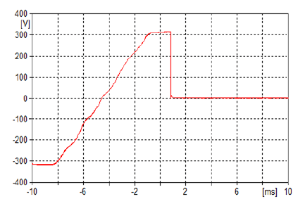
Measured waveform of voltage across the standalone mechanical switch is presented in Fig. 13.
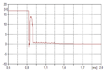
Measured current waveforms of mechanical contacts of standalone switch are presented in Fig. 14.
Calculated waveform of power led by mechanical contacts of standalone switch is presented in Fig. 15.
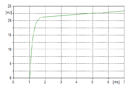
Calculated waveform of energy dissipated at mechanical contacts of standalone switch is presented in Fig. 16.
2. MOSFET solution
Measured waveform of voltage across the mechanical contacts in hybrid switch with MOSFET is presented in Fig. 17.
Waveform of voltage across the mechanical contacts in hybrid switch with MOSFET is presented in Fig. 18.
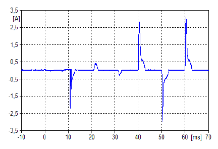
Measured current waveforms of entire hybrid switch with MOSFET component are presented in Fig. 19.

Measured current waveform of MOSFET component is presented in Fig. 20.
Measured current waveform of mechanical contacts in hybrid switch with MOSFET component is presented in Fig. 21.
Calculated power waveforms led by MOSFET component and mechanical contacts are presented in Fig. 22.
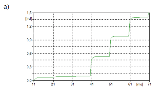
Calculated energy waveforms dissipated at MOSFET component and mechanical contacts are presented in Fig. 23.
3. Triac solution
Measured waveform of voltage across the mechanical contacts in hybrid switch with triac component is presented in Fig. 24.
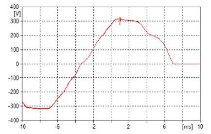


Zoomed waveform of voltage across the fast mechanical contacts in hybrid switch when triac component conducts is presented in Fig. 25.
Measured current waveforms of entire hybrid switch with triac component are presented in Fig. 26.
Measured current waveform of triac component is presented in Fig. 27.
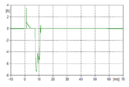
Measured current waveform of slow mechanical contacts in hybrid switch with triac component is presented in Fig. 28.
Calculated power waveforms led by triac component and mechanical contacts are presented in Fig. 29.
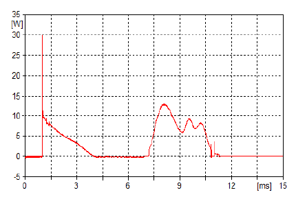
Fig.29. Calculated power waveforms: a) power at mechanical contacts; b) power at semiconductor branch – Triac solution
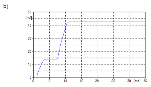
Calculated energy waveforms dissipated at triac component and mechanical contacts are presented in Fig. 30.
Analysis of obtained results
This part of paper contains comprehensive descriptions of two solid state solutions of inrush current limiting devices, dedicated for integration with LED light switches (rockers type). The principle of operation in both cases are completely different. Triac solution significantly reduces peak value of inrush current during LED’s turning-on, while MOSFET solution limits only energy dissipation during contact bouncing. In both cases, the energy dissipated at contacts is reduced, hence both lifespan of mechanical contacts as well as lifespan of entire mechanical switch are increased.
Table 1. Comparison of main features of developed solutions is presented in Tab. 1
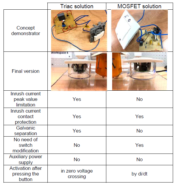
Both solutions do not need auxiliary power supply and can be connected into existing mechanical switch as extended module. The main function of the proposed solutions is to limit energy dissipated on mechanical contacts during inrush transients to eliminate undesired phenomena, such as arc erosion and contact welding that could lead to permanent damage of the mechanical switches.
Application of Triac solution requires modification of mechanical switch in comparison to MOSFET solution. However, MOSFET solution is more complex due to self-triggering principle of operation (based on di/dt detection).
The biggest advantage of the triac solution is significantly higher the efficiency for limitation of inrush current in energizing circuit.
Comparison of main features of developed solutions is presented in Tab. 1.
Detailed comparison of energy dissipation on mechanical contact, and inrush current limitation are depicted in Fig. 31 and 32.
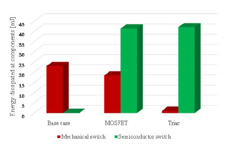

As shown in Fig. 31, the energy losses dissipated at semiconductors branches are higher than on mechanical contacts due to characteristics of semiconductor elements (on-state resistance), however during normal operation, semiconductors are bypassed by mechanical contact.
The MOSFET solution does not limit the peak value of inrush current in comparison to the base case (Fig. 32). It results from its principle of operation – where part of the energy from initial di/dt impulse is harvested and used to ignition of the MOSFET, during mechanical contacts bouncing.
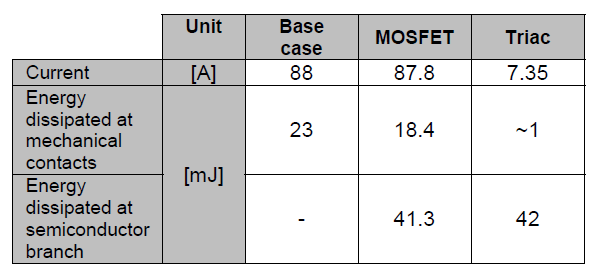
In case of Triac solution, the value of inrush current is 95% reduced in comparison to base case – what summarized in Table 2.
Table 2. Comparison of inrush peak current and calculated energies for considered cases
Conclusions
Hybrid LED light switch (mechanical switch with bypassing semiconductor circuit) may find an application in electric circuits which are being used in each branch of an industry and in residential installations, however the proper functioning of such switching apparatus strongly depends on surface conditions of electrical contacts and electrical conditions within power network. The novel circuits presented in the paper utilizes:
• triac device switched on in zero voltage which provide elimination of inrush current generated by capacitive type of the loads, as modern LED lights,
• MOSFET device absorbing significant part of the inrush current during LED lights turning on.
Compact size and simplicity of developed PCBs allows their easy integration with existing solutions. The proposed hybrid LED light switch (mechanical switch bypassed by semiconductor switch) during switching operation enables to achieve:
• arc-less switching operation,
• mitigation of switching transients,
• increased lifespan / decreased aging of contacts and the whole switch in comparison to existing mechanical switches,
• increased durability on overcurrent states in comparison to semiconductor switch,
• limited on state losses in comparison to semiconductor component.
Further development of proposed solution may provide further facilities, such as: sizing and cost optimization. Proposed solutions may be also developed for issue related to switching off circuit, which may provide complex limitation of electric arc energy both during switching-on and switching-off electrical circuits.
REFERENCES
[1] Holroyd F. W. and Temple V. A. K., Power semiconductor devices for hybrid breakers, IEEE Trans. Power Eng. Rev., vol. PER-2, no. 7, (1982), 48-49
[2] Steurer M., Frohlich K., Holaus W., Kaltenegger K., A novel hybrid current-limiting circuit breaker for medium voltage: Principle and test results,” IEEE Trans. Power Del., vol. 18, no. 2 (2003), 460-467
[3] Oramus P., Florkowski M., Rybak A., Sroka J., Investigation into Limitation of Arc Erosion in LV Switches Through Application of Hybrid Switching, IEEE Transactions on Plasma Science, vol. 45, 2017, p. 446-453
[4] Oramus P., Florkowski M., Limitation of Electric Arc Energy in LV Switches During Inductive Current Interruption, IEEE Transactions on Power Delivery, vol. 32, 2017, p. 1946-1953
[5] Van Gelder P., Ferreira J. A., Zero volt switching hybrid DC circuit breakers,” Proc. IEEE Ind. Appl. Conf., vol. 5, (2000), 2923-2927
[6] Jungblut R., Sittig R., Hybrid high-speed DC circuit breaker using charge-storage diode, Proc. IEEE Ind. Comm. Power Syst. Tech. Conf., (1998), 95-99
[7] Asplund G., Lescale V., Solver C. E., Direct-current breaker for high power for connection into a direct-current carrying highvoltage line, U.S. Patent 5 517 378, (1996)
Authors: dr inż. Mariusz Stosur, ABB E-mobility, ul. Starowislna 13A, 31-038 Krakow, Poland, E-mail: mariusz.stosur@pl.abb.com; dr inż. Kacper Sowa, ABB Electrification, ul. Starowislna 13A, 31-038 Krakow, Poland, E-mail: kacper.sowa@pl.abb.com; dr inż. Piotr Oramus ABB E-mobility, ul. Starowislna 13A, 31-038 Krakow, Poland, E-mail: piotr.oramus@pl.abb.com; dr inż. Adam Ruszczyk, ABB Electrification, ul. Starowislna 13A, 31-038 Krakow, Poland, E-mail: adam.ruszczyk@pl.abb.com; mgr inż. Pawel Aloszko, ABB Corporate Technology Center, ul. Starowislna 13A, 31-038 Krakow, Poland, E-mail: pawel.aloszko@pl.abb.com.
Source & Publisher Item Identifier: PRZEGLĄD ELEKTROTECHNICZNY, ISSN 0033-2097, R. 98 NR 7/2022. doi:10.15199/48.2022.07.20
