Published by Jakub KELLNER1, Michal PRAZENICA2, Department of Mechatroncs and Electronics, Faculty of Electrical and Information Technology, University of Zilina, Slovakia
Abstract. This article deals with the problem of elimination inrush currents. The document proposes an active method for limiting the inrush currents during circuit switching when high inrush currents occur. The proposed system limits current in the circuit by means of a series connected Mosfet transistor. The Mosfet transistor is controlled in a linear resistive region. In the case of an inrush current in a circuit, the Mosfet transistor limits the magnitude of the current flowing into the circuit. The article also solves the problem of transistor power load. In the article there is a chapter that deals with the maximum magnitude of the limiting current that can flow through the transistor so as not to destroy it. In this new inrush current limiting configuration, the operator can directly define the amount of surge current that must not be exceeded after the circuit is closed. The proposed system is also complemented by other protective and control elements that are described in this article.
Streszczenie. Artykuł dotyczy problemu eliminacji prądów rozruchowych. Zaproponowano aktywną metodę ograniczania prądów rozruchowych podczas przełączania obwodu, gdy występują duże prądy rozruchowe. Proponowany system ogranicza prąd w obwodzie za pomocą szeregowo połączonego tranzystora Mosfet. Tranzystor Mosfet jest kontrolowany w liniowym obszarze rezystancyjnym. W przypadku prądu rozruchowego w obwodzie tranzystor Mosfet ogranicza wielkość prądu wpływającego do obwodu. Artykuł rozwiązuje również problem obciążenia mocy tranzystora. W artykule jest rozdział poświęcony maksymalnej wielkości prądu ograniczającego, który może przepływać przez tranzystor, aby go nie zniszczyć. W tej nowej konfiguracji ograniczania prądu rozruchowego operator może bezpośrednio określić wielkość prądu udarowego, której nie wolno przekroczyć po zamknięciu obwodu. Proponowany system uzupełniono również innymi elementami ochronnymi i kontrolnymi opisanymi w tym artykule. Eliminacja nadmiernego wzrostu prądu rozruchowego
Słowa kluczowe: prąd rozruchowy, tranzystor Mosfet, ograniczenie, przetwornik.
Keywords: Inrush current, Mosfet transistor, limitation, converter.
Introduction
With increasing demands on the power of electric motors for various technical sectors (e.g. electric vehicles for traction purposes), the power of power semiconductor converters for connecting these motors is also increasing. As the power of the inverters increases, there is a problem with the inrush current. The problem of inrush current is compounded when using traction battery power used in cars.
The inrush current is the instantaneous input current of a high amplitude circuit that occurs when the circuit is switched on as a result of charging capacitors, inductors and transformers. This inrush current has a large amplitude and can reach currents of up to several tens of kilo-ampere [1] – [4].

Therefore, it is very undesirable in electrical circuits. In circuits where the inrush current occurs, the elimination of this undesirable phenomenon is solved by increasing the resistance in the circuit. In most cases, a resistor or an NTC thermistor is used to increase the resistance in the circuit. The duration of the inrush currents is of the order of milliseconds, the duration of this action being dependent on the size of the RC members in the circuit. Figure 1 shows an example of the current waveform when in the circuit the inrush current was generated [5] – [8].
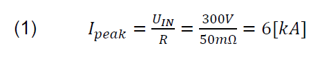
The system designed by us solves the elimination of surge currents for the 9kW inverter, which is used to power supply the asynchronous motor. Input voltage for the inverter is realized by traction batteries with nominal voltage 300V, DC. The total charge capacity in the circuit is 5mF and the parasitic resistance in the circuit is estimated at 50mΩ. In this case, the inrush current would occur during the power on the Ipeak = 6kA circuit. This is confirmed by the simulation shown in Figure 2. Since the capacitor at the moment of switching on was a short circuit, the current was limited only by the resistance in the circuit:

Due to the high inrush current, it is not suitable to use a resistor or an NTC thermistor for limitation. Therefore, we decided to design a system that uses a controlled Mosfet transistor. The advantage of this system is that we can adjust the magnitude of the inrush current. This system can also be used for other circuits that have lower voltage and current parameters for which this system was designed [9].
Inrush current limitation with Mosfet transistor
As mentioned above, the inrush current during the initial start-up of the inverter that feeds the asynchronous motor can be limited by the Mosfet transistor. A schematic diagram of this circuit is shown in Figure 3.

By controlling the transistor in its resistive area, we can reduce the magnitude of the inrush current generated by the charging of the capacitors of the inverter. This method is much more efficient and preferable than using a resistor or NTC thermistor. The advantages of this configuration are:
1.) Possibility to set maximum surge current. The user can set the amount of current which must not be exceeded. This feature allows the designed system to be used for other applications where inrush current limitation is required [10] – [12].
2.) System efficiency. Because it is a power semiconductor converter, we try to make the converter efficiency as high as possible. Therefore, the use of a resistor is not appropriate. We would reduce the efficiency of the inverter. But if we use a Mosfet transistor, we can effectively regulate the power supplied to the DC bus inverter [13].
3.) Power load of the limiting component. If we used a Resistor to limit the current, the power dissipation at the resistor would be too high.
Example of calculating instantaneous power on the limiting resistor (Pdissipation), for the proposed application: Supply voltage: UIN = 300V, DC; Circuit Capacity: C = 5mF; Limiting resistance: R = 20Ω. The effective value of the current in the circuit was: Irms = 5,9A. Power dissipation is [14]:

Power part design
Figure 4 shows a schematic of the power section of the inrush current limiting system. The power part of the proposed system consists of three main parts. These are active power semiconductor components. The main semiconductor component that provides the whole principle of inrush current limitation is Mosfet transistor. Its control ensures the limitation of the current flow in the circuit. The transistor is active in the case of over currents that occur during circuit switching on. Another element in the circuit is relay 2, which serves as a bypass member.
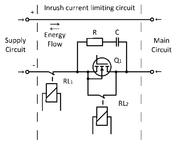
Relay 2 is connected in parallel to the transistor and at the moment the inrush current limitation is complete, relay 2 closes and the transistor is bypassed. The third active element in the power section is relay 1, which ensures the overall start and stop of the system. It also serves as a protective relay.
In the power section, an RC snubber is also contemplated to optimize the transistor to avoid failure during operation. The system can conduct current in both directions. Therefore, it is suitable for use in traction applications where we can measure and adjust the amount of current flow.
Simulation results of the proposed system
The proposed system was simulated in Matlab / Simulink environment. The simulation is based on current limitation during the initial inverter switching on. At this point, high capacity is charging. Figure 5 shows the voltage on the main circuit and the current flowing into the circuit. Using a current limiting transistor, we regulated the current in the circuit to I = 10A. Where we suppressed the current from 6kA to 10A. This, however, greatly increased the delay time τ.
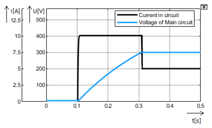
Figure 6 shows the waveforms that determine the operation of the transistor and bypass relay.
The black waveform shows the current on the transistor that limits the inrush current to 10A. The orange waveform represents the voltage across the transistor, which gradually decreases, while the voltage across the main circuit increases. The green curve represents the current through the bypass relay. We can see that if the voltage on the transistor drops to zero, the voltage on the main circuit will be equal to the supply voltage. Then the transistor turns off and the bypass relay is turned on, through which the load current flows into the circuit.
Simulation verification of transistor power load
This chapter shows the results of the transistor power load during the current limitation. In the simulation for the limitation, we detected the power losses on the Mosfet transistor at the time the transistor was in operation using the “Pe_getPowerLossSummary” function [15] – [17].
Table 1 shows the Mosfet current through the transistor, the time delay, the power dissipation on the transistor, and the energy on the transistor. The simulation input voltage is UIN = 300V. Main circuit capacity is C = 5mF.
Table 1. Transistor load simulation varication
For the measured loads and time delays, we created a graph of the magnitude of the current through the Mosfet transistor, which can be seen in Figure 7. From the waveform we can see that with increasing current the delay time decreased but the power load of the transistor increased periodically.
Using this function, we can determine the maximum current limiting magnitude for a selected Mosfet transistor so that it does not exceed its maximum permissible power load. To prevent Mosfet transistor from straining.
System verification on real sample
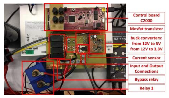
The proposed system was verified on a real sample. Measurements were performed at reduced parameters. The prototype was created for the experimental verification of system functionality. The thickness of roads and conductive connections of real sample does not correspond to the power load for which the system was designed. Therefore, all experimental measurements were verified at reduced voltage. Figure 8 shows a prototype of the proposed system. The illustration shows the description of each part of the system. The designed system was controlled by a C2000 microcontroller from Texas Instrument TMS 320F28069. Figure 9 shows the waveforms from the inrush current limitation measurement. The inrush current is limited to Ilim = 3,6A. The main circuit capacity is C = 4,2 mF. Supply voltage is UIN = 37V.
We can see from the waveform that the current in the circuit did not exceed the allowed current during charging.
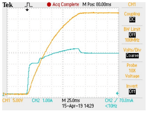
The yellow waveform represents the voltage on the main circuit. The blue waveform represents the current in the circuit. The main circuit was gradually charged to the supply circuit voltage. After the capacitor was charged, the current in the circuit remained at I = 4A. Because the main circuit was loaded with a resistance R = 9,2Ω. The time delay in the circuit was 120ms.
Figure 10 shows the waveforms of inrush current limitation of a main circuit with the following parameters: UIN = 70,5V; Rload = 39Ω; C = 2,2mF. The yellow waveform represents the voltage on the main circuit, which gradually increased to the value of the supply voltage. The blue waveform represents the voltage on the transistor. This, in turn, drops to zero. The purple waveform is the current in the circuit. The current was limited to Ilim = 1,8A. The load current in the circuit is Iload = 1,7A. The green curve represents the current through the bypass relay. From this we can see that the transistor led the current during the inrush current limitation. Then the transistor and the relay led simultaneously. And then only the bypass relay conducts current to the load.
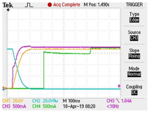
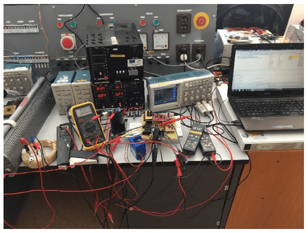
Figure 11 shows a measurement workstation consisting of a power supply, current probes, oscilloscope, multimeter, voltage probes, load resistance, load inductance, auxiliary power supplies and a notebook for communication with the microprocessor.
Conclusion
This article presents a new design of the inrush current limiting system. It is an effective way of limiting. In the proposed system there is the possibility to specify the magnitude of the maximum inrush current. Therefore, the system can be used for various applications. Current limitation is solved with Mosfet transistor, which provides considerable advantages over conventional methods of limiting inrush current. The proposed system was verified by simulation and on a real sample. Results from simulations and measurements are presented in this article. From the results we can see that the proposed system successfully limits the magnitude of the inrush current during the initial switching on of the main circuit.
Acknowledgement This work was supported by projects: Vega 1/119/18 Research of the methodology for optimization of EMC of WPT systems, ITMS 26210120021.
LITERATURA
[1] J-Ch. Wu, H-L. Jou, K-D Wu, N-T Shen, Hybrid Switch to Suppress the Inrush Current of AC Power Capacitor, IEEE Transaction on Power Delivery, vol. 20, n. 1, pp. 506-511.
[2] T. Jiang, P. Cairoli, R. Rodrigues, Y. Du, (2017). Inrush current limiting for solid state devices using NTC resistor. SoutheastCon 2017. doi:10.1109/secon.2017.7925398.
[3] Iuga, B., & Tirnovan, R. A. (2019). Step by step Limiting for Capacitors Inrush Current Used in Voltage Power Supplies. 2019 8th International Conference on Modern Power Systems (MPS). doi:10.1109/mps.2019.8759664.
[4] H. Suryoatmojo, M. Ridwan, I. Izzatur Rahman, D. Candra Riawan, M. Ashari, Design of Bidirectional DC-DC Cuk Converter for Testing Characteristics of Lead-Acid Battery, Przeglad Elektrotechniczny, doi:10.15199/48.2020.03.26.
[5] R. Araria, K. Negadi, M. Boudiaf, F. Marignetti, Non-Linear Control of DC-DC Converters for Batery Power Management in Electric Vehicle Application, Przeglad Elektrotechniczny, doi:10.15199/48.2020.03.20.
[6] G. Mallesham, K. Anand, Inrush Current Control of a DC/DC Converter Using MOSFET, International Conference on Power Electronic, Drives and Energy Systems 2006, India.
[7] K. Praveen, N. Kulshrestha, L. Srivani, D. Thirugnanamurthy, B. K. Panigrahi, Prognostics of Electrolytic Capacitors under Inrush Current Overstress, International Conference on Smart City and Emerging Technology (ICSCET) 2018, India.
[8] Eun-Ju Lee, Jung-Hoon Ahn, Seung-Min Shin, Byoung-Kuk Lee, Comparative analysis of active inrush current limiter for high-voltage DC power supply system, 2012 IEEE Vehicle Power and Propulsion Conference.
[9] M. Frivaldsky, P. Špánik, J, Morgos, M, Pridala, Control strategy proposal for modular architecture of power supply utilizing LCCT converter, Energies, Vol. 11, N. 12, 2018, Article Number: 3327.
[10] Gonthier, L., & Renard, B. (2015). AC/DC reversible mixed inverter with built-in inrush-current limitation and cut-off standby losses. 2015 17th European Conference on Power Electronics and Applications (EPE’15 ECCE-Europe). doi:10.1109/epe.2015.7309066.
[11] K. Dabala, M. P. Kazmierkowski, Converter-Fed Electric Vehicle (Car) Drives, Przeglad Elektrotechniczny, doi:10.15199/48.2019.09.01.
[12] M. Frivaldsky, J, Morgos, B. Hanko, Start-up power supply for automotive applications, International Conference Elektro 2018, CZ.
[13] Madani, S. M., Rostami, M., Gharehpetian, G. B., & Haghmaram, R. (2012). Inrush current limiter based on threephase diode bridge for Y-yg transformers. IET Electric Power Applications, 6(6), 345. doi:10.1049/iet-epa.2011.0317.
[14] H. Hoshi, T. Tanaka, M. Noritake, T. Ushirokawa, K. Hirose, M. Mino, Consideration of Inrush Current on DC Distribution System, Proceedings of Intelec 2012, USA.
[15] J.K. Kim, S. S. Lee, W-S. Oh, J-E. Kim, G-W. Moon, Ch-H. Gil, J-R. Cho, Start- up inrush current reduction technique of asymmetrical half-bridge DC/DC converterfor PC power supply, 7th Internatonal Conference on Power Electronics, 2007, South Korea.
[16] J. Sedo, S Kascak, Control of single-phase grid connected inverter system, International Conference Elektro 2016, Slovakia.
[17] B. Dominikowski, Inteligentne pomiary szybkozmiennego prądu akumulatora trakcyjnego pojazdu elektrycznego wykorzystujące interwałowe zbiory rozmyte typu-2 o wnioskowaniu Takagi-Sugeno-Kanga, Przeglad Elektrotechniczny, doi:10.15199/48.2019.11.12.
Authors: Ing. Jakub Kellner was born in 1995 in Kezmarok, Slovakia. He is graduated at the University of Zilina (2019) in Power Electronics. He is currently an internal PhD student at the University of Zilina – Department of Mechatronics and Electronics in the power electrical engineering study program. The main research interest is about power electronic systems.
Ing. Michal Prazenica, PhD was born in 1985 in Zilina, Slovakia. He is graduated at the University of Zilina (2009). He received the Ph.D. degree in Power Electronics from the same university in 2012. He is now Research worker at the Department of Mechatronics and Electronics at the Faculty of Electrical Engineering, University of Zilina. His research interest includes analysis and modelling of power electronic systems, electrical machines, electric drives, and control.
Source & Publisher Item Identifier: PRZEGLĄD ELEKTROTECHNICZNY, ISSN 0033-2097, R. 96 NR 8/2020. doi:10.15199/48.2020.08.20
