Published by Adam RUSZCZYK1, Krzysztof KÓSKA1, Konrad JANISZ2
ABB Corporate Research Centre, Poland (1), AGH University of Science and Technology, Poland (2)
Abstract. This paper describes new concept of a switch dedicated for control of three-phase capacitor bank used for low voltage, reactive power compensation. The proposed device utilizes fully controlled IGBT transistors that gives possibility to break capacitor current in moment that ensures zero voltage remaining on capacitor’s terminals. This minimize voltage stress for switch and capacitor as well as allows to turn-on again capacitors bank without unnecessary delay. This paper describes structure of hybrid switch and its operation with capacitor bank and detuning inductor.
Streszczenie. Artykuł opisuje nową koncepcję łącznika dedykowanego do załączania banku kondensatorów używanych do kompensacji mocy biernej w sieciach niskiego napięcia. Zaproponowany łącznik wykorzystuje tranzystory IGBT, co umożliwia przerywanie prądu kondensatora w chwili, gdy napięcie na zaciskach kondensatora jest równe zero. Zmniejsza to stres napięciowy łącznika i kondensatora oraz pozwala na ponowne załączenie banku kondensatorów bez zbędnego opóźnienia. Artykuł opisuje strukturę łącznika hybrydowego oraz jego pracę z bankiem kondensatorów i dławikiem wygładzającym. (Łącznik półprzewodnikowy dla kondensatorów używanych w kompensatorach mocy biernej).
Keywords: Solid-state switch, Active clamping protection circuit, Reactive power control.
Słowa kluczowe: Łącznik półprzewodnikowy, Układ aktywnego ograniczenia napięcia Sterowanie mocą bierną.
Introduction
The circulation of the reactive power in the system causes different types of power quality effects therefore the generation of reactive power by consumers is restricted by the electricity supplier. The inductive power generation in the most cases is compensated by attaching capacitor banks. It is very simple, inexpensive and effective way of compensation. The drawback of the method is that the reactive power compensator (RPC) cannot compensate reactive power in continuous way due to a discrete value of the capacitors. The typical approach to solve this inconvenience is to split total capacitance of reactive power compensation (RPC) system into smaller blocks that can be simply connected or disconnected to the grid in order to match the needed capacitive power [1], [2].
The most common RPCs use electromagnetic relays to switch capacitor banks. One of the advantages of relays is low contact resistance, and thus low conduction power losses. On the other hand electromagnetic relays have undetermined operational delay and there is no possibility to synchronize them with zero crossing of the voltage. As a result large inrush currents occurs during connection of capacitor to the grid. Typical approach to this problem is utilization of auxiliary contacts with initial pre-charge resistors which are bypassed by main contacts for normal operation. This simple solution damps current to smaller values, but it is far from ideal because inrush current still exists [3].
A much more elegant solution uses solid-state switches (thyristors) as a replacement for relays. Firstly, the moment of turn-on of a semiconductor switch can be precisely controlled at the moment of the zero-voltage crossing [4]. Secondly, thyristors are characterized by relatively low forward voltage drop (approximately 1,5V) and, in consequence, low conduction losses in comparison to the other semiconductor components that are able to withstand voltage higher than 1,4kV. One of the thyristor’s drawback is its lack of turn-off capability. Silicon Controlled Rectifier (SCR) commutates when conducted current drops below, so called, holding current. In AC grid, a capacitive load is turned off during zero crossing of the current and hence peak value of the voltage. Because of voltage remaining across the capacitor, in the following grid voltage period, stress across the thyristor can reach approximately twice phase-to-phase peak voltage.
In this paper the new hybrid, IGBT based, three-phase switch is presented. Presented switch can break current of capacitor in its peak value that corresponds to zero voltage remaining at the capacitor.
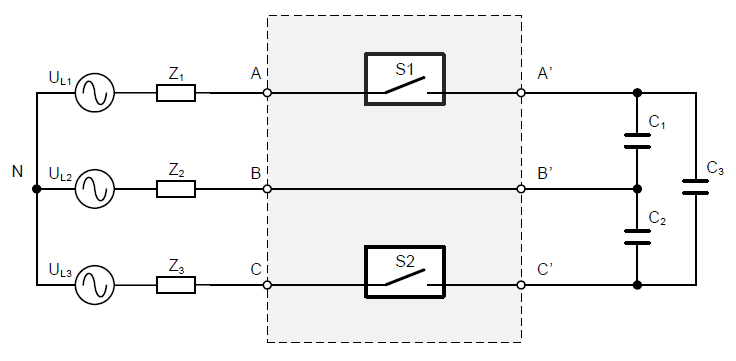
Switching device is dedicated for three phase compensator bank. It comprises two physical switches (Fig.1) which break currents in two phases. This is enough to disconnect or connect three-phase delta-connected capacitor bank. Both switches comprises bidirectional solid-state switches and electromechanical relays connected in parallel (Fig. 2). Similar hybrid solutions are commonly utilized in applications where high conduction losses are not acceptable [5], [9].
Hybrid solution combines benefits of a relay (low conduction losses) and semiconductor (synchronized turn- on and -off, as well as arc-less operation). The drawback is slightly increased cost and complexity of the device. Three phase switch, presented in Fig.1 and Fig.2, enables a connection of the capacitor bank without inrush current. The same switch is able to disconnect capacitors bank in a manner that afterwards all three capacitors are completely discharged (Fig.6). This result can be achieved by use of fully controlled switches S1 and S2 that can break capacitors’ currents in specific moments.
Significant problem appears when compensating capacitors are connected to a distorted grid. In that case the capacitor creates low impedance path for high-order harmonic current flow. It’s dangerous phenomenon which may cause serious consequences in the power quality. To avoid such situation the detuning inductors are connected in series with capacitor bank (more details are described in the Section – Filtering of high-order harmonics).
The overvoltage spikes are generated during the disconnection process of the capacitor by interruption of the current in the circuit with additional detuning inductance. It has destructive influence on the semiconductor switch with IGBT component. In order to prevent break-over of the transistor, active clamping circuit is proposed and described in Section – Overvoltage inducted during current interruption.
Thyristors based solid-state switch for capacitor bank
The result of operation of the three-phase switch based on thyristors components is presented in Fig. 3. Capacitor switch is composed of two independent physical switches (Fig.1). Both physical switches are made of two antiparallel connected thyristors in order to form a bidirectional valve. S1 and S2 work independently and are turning-on when the voltage seen across the switch is crossing zero value. The consequence of this fact is that the physical switches works in sequence. This ensures that the capacitor bank can be connected without inrush current. Moreover, transient states observed in phase currents are greatly reduced in comparison with electromechanical relay solution.
The commutation delay between S1 and S2 equals 90 deg. (5ms) for both turn-on and turn-off operation. It may look odd that phase delay between two switches in three-phase circuit is exactly 90 deg. (5ms) neither 60 nor 120 degrees. The reason of a such behavior is explained on voltage graphs shown in Fig. 4
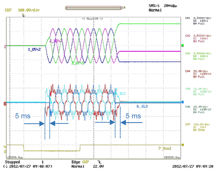
Let’s assume that both switches S1 and S2 are in blocking condition of phase-to-phase voltages UL12, UL32 respectively. All capacitors are discharged. Let’s start with S1 closing it at first the zero crossing of the voltage UL12. Then capacitors C1, C2 and C3 are charged up. In series connected capacitors C2 and C3 create parallel branch to C1 and form a voltage divider for UL12 voltage. During this period switch S2 is connected between phase UL3 and midpoint of UL12 voltage. This voltage is in phase to UL3, but its amplitude is √3/2 higher according to height of an equilateral triangle created by phase-to-phase voltages (Fig.4).

Switch-off process is analogical to switch-on, but the difference is that non-zero voltages remain at capacitors terminals afterwards. In the following grid period (20ms) switch has to withstand sum of grid amplitude voltage and capacitor’s voltage. In consequence of it switches and capacitors have to be rated for higher voltage that makes a practical system more expensive. This problem is unsolvable with use of thyristors components for solid-state switch because they break capacitors’ current near zero current condition, so maximum voltage. This situation is presented in Fig.3.
IGBT based solid-state switch for capacitor bank
Proposed solution uses IGBT instead of thyristors. To achieve bidirectional operation transistor is connected with single phase diode bridge (see Fig. 2 and Fig.12). IGBT is turned-on exactly like thyristor at zero crossing of the voltage. This prevents an occurrence of inrush current. But unlike thyristor, the
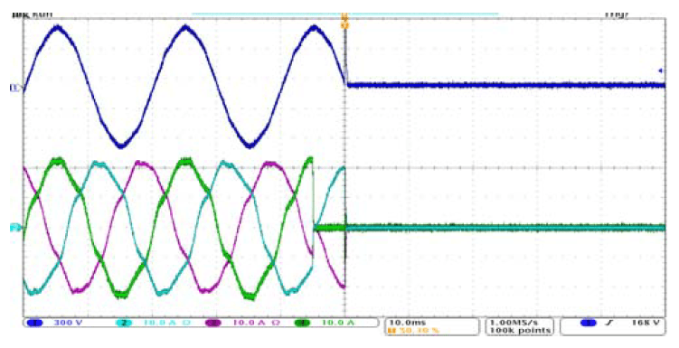
IGBT is turned-off in the moment when voltage, which is measured at selected capacitor, is close to zero. The switch, which operation is based on the described principles has been designed and tested. It proves that operation of two physical switches is enough to achieve zero voltage across capacitors after turnoff. This device is presented in Fig.5. In parallel to IGBT based switches electrometrical relays are connected.
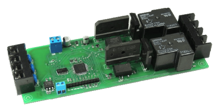
Presented hybrid switch is equipped with a simple control logic implemented on CPLD which is responsible for synchronization with the grid and generation of control signals for IGBTs and relays.
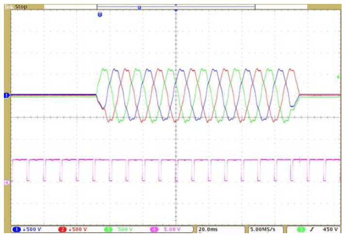
The turn on-off operation of the switch is presented in Fig.6. It presents capacitor voltages. One can observe that capacitors are discharged before and after operation of the switch. That definitely reduces voltage stress at capacitors and switches after disconnection. Moreover, it is not necessarily to wait until capacitors will be discharged before next operation. User is able to turn on the capacitor bank again without time restrictions. Dynamics of the presented hybrid solution is comparable with thyristor-based switch.
The consequence of capacitor turn-off with zero voltage condition is interruption of non-zero current. Capacitor’s current waveforms during disconnection are presented in Fig.7. In ideal condition, when current is interrupted in a circuit that has only capacitive character the current can be interrupted immediately. The current interruption in a circuit where even the smallest inductance exists a voltage spikes will be induced.
Filtering of high-order harmonics
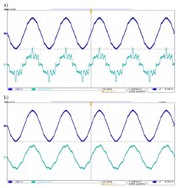
The known problem with capacitor attached to the distorted network is a generation of high-order harmonics of current. This problem exists no matter of type of used switch technology: electromechanical, thyristor or IGBT. Line current of single-phase of R
load with purely capacitive compensator is presented in Fig.8a. The reactive power compensation reduces reactive power flow for fundamental harmonic but at the same time increase high-order current harmonics. Because of existence of the line impedance the distorted current causes the additional voltage drop that increases voltage distortions.
The solution is to use of detuning inductor installed in series with capacitor bank. Properly selected detuning inductor causes smoothing the capacitor current. This effect can be observed in Fig.8b.
This justifies the necessity of use of detuning inductor. Detuning inductance L connected in series with compensating capacitor C creates series resonant circuit with a resonant frequency below the 5th (or 3rd) order harmonic, which is the most common in a harmonic-rich environment. In Europe, detuning by a factor of 3.78 (7%) times the line frequency is most common, whereas in other parts of the world, in particular in Asia, a factor of 4.08 (6%) is more often selected. For high demanding systems 2,83 (12,5%) or even 2,67 (14%) factor is used.
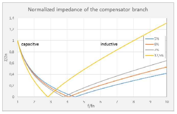
To fulfill resonance frequency requirements each capacitor bank in RPC must be equipped with separated detuning reactor with properly selected detuning inductance. As it is shown in Fig.9, the LC filter operating below resonant frequency is in capacitive mode and above it in inductive mode.
Overvoltage inducted during current interruption
The detuning inductor is an effective solution for high order harmonics rejection. However, existence of additional inductance in series with compensating capacitor creates serious problem for IGBT-based switch. During interruption of the current an overvoltage is inducted which can break over the structure of semiconductor. Every physical circuit has small inductance introduced by connection wires, so even a lack of detuning inductor do not allow to neglect this problem. Fig.10 shows two examples of line current without (Fig.10a) and with detuning inductor (Fig.10b).
In Fig.10b the effectiveness of higher harmonics filtration can be observed when detuning inductor is used. In Fig.10a short voltage spikes of few microseconds duration are visible even with lack of detuning inductor. In both cases the overvoltage spikes were limited by the surge arresting circuit which protects IGBTs.
The most common overvoltage protection device is metal oxide varistors (MOV’s). Although MOV seems to be good solution in many applications, the utilization in IGBT based switch is far from ideal.
MOV are dedicated for incidental operation as a surge arrester. The structure of metal-oxide degrades with every action cause degradation in the metal oxide material, which eventually leads to component failure. Theoretically, according to [10] low energy pulses can be suppressed infinitive number (Fig.11). But it is hard to ensure that the current magnitude and time duration will remain unchanged when the impedance of compensating branch may vary due to a capacitance and inductance change. Therefore the operating point for MOV can be moved into limited lifespan region (Fig.11).
Because varistors only dissipate a relatively small amount of average power they are not suitable for repetitive applications that involve substantial amounts of average power dissipation.
Additional limiting factor is ambient temperature that forces derating of surge power. To ensure long time of trouble less operation for solid-state switch the size of MOV has to be carefully selected. For the most cases it means the MOV has to be oversized.
In solid-state switch the overvoltage is present during every turn-off of IGBT, so after limited number of cycles MOV may fail. In this paper it is proposed to use transistor active clamping circuit, in which IGBT tries to protect itself by reducing di/dt of interrupted current in order to limit induced voltage to the safe level. This system is described in next chapter.
Transistor Active clamping circuit
Break of the load current in inductive circuit generates voltage equal UL=–L(diL/dt). It means that derivative of the current has to be limited to keep induced voltage below maximal. It is achieved by additional circuit composed of in series connected high voltage Zener diodes (Fig.12) connected between IGBT’s emitter and gate terminals.
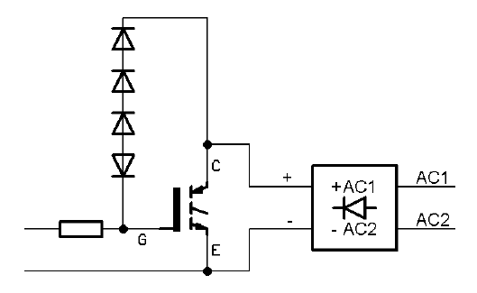
This kind of protection circuit is commonly used with high power IGBT transistors [7], [8]. When IGBT is turning off an inductive load and inducted voltage UL exceeds the voltage threshold set by Zener diodes and the IGBT is driven back into conductive state by current injected into the gate. In fact IGBT remains in active state during current interruption and can be interpreted as variable resistance. The main drawback of this method is that all energy stored in inductance has to be intercepted by internal IGBT silicon structure.
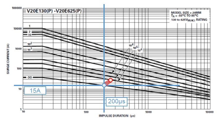
In the laboratory setup with three capacitors 62μF in delta connection (Qc = 10 kvar @ ULL= 400Vac, f = 50Hz) to achieve 7% detuning reactance three phase choke has been used. Nominal inductance of this choke is 3,84mH per phase. Laboratory verification was made by interruption of instantaneous current of 27A. Worse switching condition has switch S2 that has to interrupt current flowing through in series connected inductances in phase L2 and L3. The energy stored in both inductances can be calculated as:
where: i – interrupted current, L – detuning inductor.
While the energy absorbed by silicon is an integral of a product of collector current IC and transistor voltage UCE in period of 220μs read from Fig.13
where: IC – collector current of transistor, UCE – voltage cross CE junction, Δt – current interruption period.
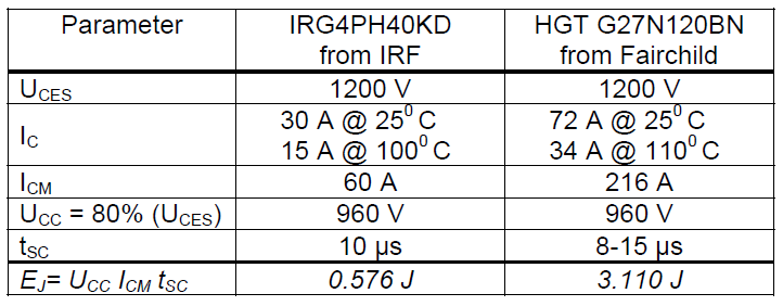
All energy stored in circuit inductances has to be intercepted by transistor (EL≈ET). Therefore a special type of transistors should be selected. According to the datasheets [11,12] for two type of investigated IGBT’s the maximal acceptable energy is calculated in Table 1.
Table 1. The IGBT parameters comparison
The discharge of energy of inductance in the IGBT transistor takes about 220μs. It is definitely too short to transfer any heat outside. The process can be treated as adiabatic. The thermal image (Fig.14) confirm that there is no visible increase of transistor’s temperature.
The HGTG27N120BN has approximately 0,036g of silicon [13]. Specific heat of the silicon equals 0,7 J/(goC). Thus, the temperature rise of the silicon equals approximately 110oC. Fortunately, heat transfers to the copper lead frame of the transistor with relatively short time constant. Copper weights 4,0g [13]. That for specific heat capacitance of copper equal 0,386 J/(goC) gives 1,57 J/oC thermal capacitance of transistor in TO-247 package. In other words a single portion of 2,8 J of energy from detuning inductor would cause increase temperature of transistor about 1,78oC. Even the turn on/off cycle realized every second cannot increase significantly temperature of IGBT enclose.
Conclusion
Paper presents a new concept of hybrid switch which is dedicated for capacitive reactive power compensator. Single device is made of two physical switches installed in two phase lines. It has been experimentally proven that proposed switch is able to disconnect a delta connected capacitor bank in manner that afterwards all three capacitors are completely discharged. Moreover it has been showed that conduction losses can be reduced by introducing hybrid solution with parallel electromechanical relay.
Finally the IGBT overvoltage protection allows to use the presented switch in RPC systems with detuning inductors.
REFERENCES
[1] Gos z towt W.: “Gospodarka elektroenergetyczna w przemyśle”. Warszawa WNT, 1973
[2] Nar tows ki Z. Baterie kondensatorów do kompensacji mocy biernej. Warszawa WNT, 1967
[3] Application Guide: Contactors for capacitor switching, 1SBC101140C0203 2009 ABB
[4] Olivier G., Mougharbel I., Dobson-Mack G.: “Minimal transient switching of capacitors”, IEEE Trans. on Power Delivery, vol. 8, no. 4, 1993, pp. 1988-1994.
[5] Bachman P.: “Crydom RHP Series – 3 Phase Hybrid Solid State Contactor”, White Paper CRYDOM Inc. 2009
[6] Ironcore – Reactors Catalogue http://www.mangoldt.com/pdf/ HvM_Ironcore_Reactors_Catalogue_2011_ENG.pdf
[7] Garcia O. , Thalheim J . , Meili N. : “Safe Driving of Multi-Level Converters Using Sophisticated Gate Driver Technology”, PCIM Asia, June 2013.
[8] Bur khard B. : “Switching IGBTs in parallel connection or with enlarged commutation inductance”, PhD thesis, Bochum 2005
[9] Shukla A., Demetriades G. D.: “A Survey on Hybrid Circuit-Breaker Topologies”, IEEE Trans. on Power Delivery, Vol. 30, No. 2, April 2015, pp. 627-641
[10] Metal-Oxide Varistors (MOVs) – UltraMOVTM Varistor Series – © 2015 Littelfuse, Inc. – Specifications Revised: 08/20/15
[11] IRG4PH40KD – Insulated gate bipolar transistor with ultrafast soft recovery diode – datasheet
[12] HGTG27N120BN – 72A, 1200V. NPT Series N-Chanel IGBT
datasheet – obsolete product.
[13] AN-7516 – Safe Operating Area Testing Without A Heat Sink
Authors: dr inż. Adam Ruszczyk, ABB Corporate Research Center, ul. Starowiślna 13A, 31-038 Kraków, Poland, E-mail: adam.ruszczyk@pl.abb.com; mgr inż. Krzysztof Kóska, ABB Corporate Research Center, ul. Starowiślna 13A, 31-038 Kraków, Poland, E-mail: krzysztof.koska@pl.abb.com; inż. Konrad Janisz, Akademia Górniczo-Hutnicza,
Source & Publisher Item Identifier: PRZEGLĄD ELEKTROTECHNICZNY, ISSN 0033-2097, R. 91 NR 12/2015. doi:10.15199/48.2015.12.03
